The George Washington
University
School of Engineering
and Applied Science
Department of Electrical
and Computer Engineering
ECE 20 - Summer 2001
Experiment # 8
MOSFET as an Amplifier
Equipment:
You must make up a complete equipment
list and have your instructor review it before you start.
Objectives:
-
To verify the operating point for a
MOSFET biasing network
-
To verify the small signal performance
for a given Common Source amplifier: RIN, ROUT, Av, Ai , maximum input
amplitude without distortion vin max , etc.
-
To verify the small signal performance
for a given Common Drain amplifier: RIN, ROUT, Av, Ai , maximum input amplitude
without distortion vin max , etc.
-
To establish the relationship between
the voltage gain and the load
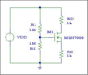
Figure # 1
1.- (HW)
DC Analysis
-
Analyze the circuit shown in Figure
# 1 (use nominal values) and find VGG, VG, VS, VD, and ID (assume VDD =
30 Volts DC, K = 40 mAmp/Volt , Vth = 1.73 V).
-
Assemble this circuit on ORCAD and perform
a bias point detail analysis. Show the appropriate voltages and current
on the schematic.
2.- DC Bias Verification
-
Build and fully test the circuit shown
in Figure #1. Measure VG, VS, VD, and ID.
3.- (HW)
Small Signal Analysis
For the circuit in Figure # 1:
-
Assuming that this circuit is operated
in Common Source (with shorting capacitor on the Source):
-
Find ROUT, RIN, Avo, Av @RL=ROUT and
Ai@ RL=ROUT. Label this as "Analysis for Common Source"
-
Also, find the maximum input voltage
vin max that the amplifier can accept before the output distorts (loaded
and unloaded).
-
Use ORCAD to find Av@RL=ROUT and Ai@RL=ROUT.
-
Assuming that this circuit is operated
in Common Drain (with shorting capacitor on the Drain):
-
Find ROUT, RIN, Avo, Av @RL=ROUT and
Ai@RL=ROUT. Label this as "Analysis for Common Drain"
-
Also, find the maximum input voltage
vin max that the amplifier can accept before the output distorts (loaded
and unloaded).
-
Use ORCAD to find Av@RL=ROUT and Ai@RL=ROUT.
4.- Small Signal Verification
Build and fully test the circuit
shown in Figure #1. By applying a sinusoidal signal such that the small
signal approximation holds, measure:
-
For the CSC:
-
RIN (input impedance) and ROUT (output
impedance) of the assembled circuit.
-
Voltage gain Av the assembled circuit
for the unloaded case (RL really large). Print the output plot and
label it as "Avo for Common Source"
-
Voltage Gain for RL equal to 2*ROUT,
ROUT, ROUT /2, and ROUT /4. DO NOT print the output plots.
Put the corresponding values of Av in a table. Label it as "Table
1 - Common Source Av for various RL"
-
Find the maximum input voltage that
the amplifier can accept before the output distorts @ RL = ROUT. Plot the
output signal and the corresponding input.
-
Determine the phase relationship between
the input and output voltages.
-
Compare the measured results to your
analysis calculations.
-
For the CDC:
-
RIN (input impedance) and ROUT (output
impedance) of the assembled circuit.
-
Voltage gain Av the assembled circuit
for the unloaded case (RL is really large). Print the output plot
and label it as "Avo for Common Drain"
-
Voltage Gain for RL equal to 2*ROUT,
ROUT, ROUT /2, and ROUT /4. DO NOT print the output plots.
Put the corresponding values of Av in a table. Label it as "Table
2 - Common Drain Av for various RL"
-
Find the maximum input voltage that
the amplifier can accept before the output distorts @ RL = ROUT. Plot the
output signal and the corresponding input. Label the plot appropriately.
-
Determine the phase relationship between
the input and output voltages.
Compare the measured results to
your analysis calculations.
Hint: Connect a large capacitor
between VCC and ground in order to reduce the noise from the source. The
noise is amplified and mixes with the output due to the input AC signal
(Vs).
5.- Conclusion
a.Considering that these
amplifiers are quite typical, what can you say about Rin, Rout, and the
Av for the Common Source and Common Drain amplifiers.
b.Based on your observation,
what are the primary differences between BJT and MOSFET Amplifiers?
c.Which configuration
is better for the voltage amplification stage in your audio mixer project:
Common Emitter or Common Source? Explain.