The George
Washington University
School of Engineering
and Applied Science
Department of Electrical
and Computer Engineering
ECE 20 - Summer
2000
Experiment # 6
BJT Detailed Analysis
on
Common Emitter
and Common Collector
Equipment:
You must make up a complete equipment
list and have your instructor review it before you start.
Objectives:
-
To analyze and verify the small signal
performance for a given Common Emitter amplifier: RIN, ROUT, Av, Ai , maximum
input amplitude without distortion and general characteristics of CE.
-
To analyze and verify the small signal
performance for a given Common Collector amplifier: RIN, ROUT, Av, Ai ,
maximum input amplitude without distortion and general characteristics
of CC.
-
To establish the relationship between
the voltage gain and the load.
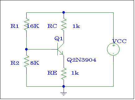
Figure # 1
1.- (HW)
CEC Analysis
In Exp. #5, the DC Bias Analysis
and general formula for Unloaded Voltage Gain (Avo) for circuit of Figure
#1 were conducted. The more detailed analysis analysis on Common
Emitter Amplifier for this circuit will be conducted in this section.
When this circuit is operated in
CEC:
-
Find ROUT
-
RIN
-
Unloaded Voltage Gain, Avo
-
Av (RL=ROUT)
-
Ai (RL=ROUT).
-
Maximum input voltage vin max that the
amplifier can accept before the output distorts (Unloaded case).
To get a credit for this analysis, you must show all the steps below:
1. Do DC Bias Analysis
2. Draw Small Signal Equivalent circuit for CEC
3. Find Rin, then Rout @Vin=0
4. Find Vout and Vin to get Av
5. Find Av @ RL=Rout
6. Find Ai
7. Find Vinmax
2.- CEC Verification
Build and fully test the circuit
shown in Figure #1. By applying a sinusoidal signal such that the small
signal approximation holds, measure:
-
RIN (input impedance) and ROUT (output
impedance) of the assembled circuit.
-
Unloaded Voltage gain, Avo. Label
the plot - "Plot 2a - Avo for CEC"
-
Voltage Gain for RL equal to 2*ROUT,
ROUT, ROUT /2, and ROUT /4. Print the output plot for each RL and
label each of plot as Plot 2b - "Av @ RL=__ for CEC"
-
Find the maximum input voltage that
the amplifier can accept before the output distorts (Unloaded case). Print
the plot and label it as "Plot 2c - Vin max before output distorts for
CEC"
-
Determine the phase relationship between
the input and output voltages.
3.- (HW)
CCC Analysis
In Exp. #5, the DC Bias Analysis
and general formula for Unloaded Voltage Gain (Avo) for circuit of Figure
#1 were conducted. The more detailed analysis analysis on Common
Collector Amplifier for this circuit will be conducted in this section.
When this circuit is operated in
CCC:
-
Find ROUT
-
RIN
-
Unloaded Voltage Gain, Avo
-
Av (RL=ROUT)
-
Ai (RL=ROUT).
-
Maximum input voltage vin max that the
amplifier can accept before the output distorts (Unloaded case).
To get a credit for this analysis, you must show all the steps below:
1. Do DC Bias Analysis
2. Draw Small Signal Equivalent circuit for CCC
3. Find Rin, then Rout @Vin=0
4. Find Vout and Vin to get Av
5. Find Av @ RL=Rout
6. Find Ai
7. Find Vinmax
4.- CCC Verification
Build and fully test the circuit
shown in Figure #1. By applying a sinusoidal signal such that the small
signal approximation holds, measure:
-
RIN (input impedance) and ROUT (output
impedance) of the assembled circuit.
-
Unloaded Voltage gain, Avo. Label
the plot - "Plot 4a - Avo for CCC"
-
Voltage Gain for RL equal to 2*ROUT,
ROUT, ROUT /2, and ROUT /4. Print the output plot for each RL and
label each of plot as Plot 4b - "Av @ RL=__ for CCC"
-
Find the maximum input voltage that
the amplifier can accept before the output distorts (Unloaded case). Print
the plot and label it as "Plot 4c - Vin max before output distorts for
CCC"
-
Determine the phase relationship between
the input and output voltages.
5.- Conclusion
-
What can you say about the general characteristics
of CEC amplifier( Rin, Rout, Av, Ai etc).
-
What can you say about the general characteristics
of CEC amplifier( Rin, Rout, Av, Ai etc).
-
Compare the measured results to your
analysis for both CE and CC. Explain any differences.
-
Why is there a difference between the
value the function generator was set for and the actual input signal?