The George Washington University
School of Engineering and Applied Science
Department of Electrical and Computer
Engineering
ECE 20 – Spring 2003
Experiment # 1
Solid
State Diodes
Testing & Characteristics
Equipment:
You must make up a complete equipment list and have your instructor review it
before you start.
Components:
- D1 - 1N34 Germanium Diode
- D2 - 1N4002 Series Silicon Diode
- DS1 - MV5753 Gallium Arsenide Phosphide (GaAsP) Red LED
- VR1 - 1N751 Zener Diode
- R1 - 1 Ohm
- R2 - 1 MOhm
- C1 - to be determined (large)
Objectives:
- To use an ohm meter to determine the forward and reverse resistance of different types of diodes
- To use the Diode Test function of the Keithley Model 175
- To obtain one diode i-v characteristic curve by using the information obtained from a test circuit
- To obtain the i-v forward bias characteristic curves for several types of diodes by using a the Tektronix Model 571
- To obtain the i-v reverse bias characteristic curve for a Zener diode
- To determine the value of the small signal resistance of one diode for different operating points and using three different techniques: graphically, analytically and by the application of a small signal.
- To appreciate the limitations of the small signal analysis technique
- To interpret the results of static and dynamic diode tests
1.- Data & Static Diode Tests
- (HW) Draw and name the electrical symbols for D1, D2, VR1 and DS1. Prepare Table # 1 to show technical information for the different diodes.
- Set the ohm meter to the appropriate range, measure and record the forward direction resistance (Rf) of D1, D2, VR1 and DS1. Then set the ohm meter to its highest scale, measure and record the reverse direction resistance (Rr) of D1, D2, VR1 and DS1. Calculate the back to front ratio (Rr/Rf) for D1, D2, VR1 and DS1. Place this information in Data Table #2.
- Set the Keithley Model 175 to perform the diode test function. Measure and record the forward and reverse bias voltage readings for D1, D2, VR1 and DS1. Place this information also in Data Table #2.
2.- Reverse Saturation Current
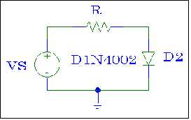
Fig # 1
Construct the circuit depicted in Fig # 1 using the following specifications:
VS = -10 Vdc
R = R2
D = D2
The Anode of D2 should be connected to R.
- Find the reverse saturation current IS of the diode. The DMM must be connected in such a manner that its loading effect is reduced to a minimum.
- (HW) What is the value of IS that SPICE uses to model this diode?
3 .- Forward i-v Characteristic
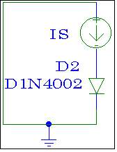
Fig # 2
- (HW) With the help of SPICE (ORCAD), plot the i-v characteristic for the D1N4002. The suggested current range is 0 to 20 mA DC. The suggested voltage range is 0 to 1 Volts DC. Label this plot as Plot # 1.
- Assemble the circuit shown in Fig # 2. Take enough current voltage measurements to plot an i-v characteristic curve for D2 (Plot 2). You will have to vary Is in order to do this. The suggested current range is 0 to 20 mA DC in 2 mA steps.Mark the point on the i-v curve that indicates the voltage drop across D2 when the forward current is equal to 10 mA DC.
- In the forward region the i-v relationship is closely approximated by:
i = IS(exp(v/nVT)-1) ------ (equation 1)
Determine the values of n and IS for
this equation to predict the same voltage values as those measured in part b)
for i =6 mA and i =14 mA.
- With the help of QUATRO or EXCEL, plot the i-v characteristics using n and IS values predicted by equation 1. Label this as Plot 3.
- Compare the value of IS obtained in part 3 c) with the value obtained in part 2.
4.- Diode Parameters on the Curve Tracer
- Use the Tektronix Model 571 Curve Tracer to obtain the i-v forward bias characteristic curves for D1, D2, VR1 and DS1. Annotate the10mA point on each curve (cut-in or cut-off point), and the point for which the voltage is equal to the value measured using the Keithley 175 diode test function. Make sure that you label the each printouts according to the diode type. For example for D1, label the printout as "I-V Forward Characteristics of D1".
- Use the Tektronix Model 571 Curve Tracer to obtain the i-v reversed bias characteristic curves for D1, D2, VR1 and DS1. On the curve for VR1 find VZ when IZ is equal to 20 mA. Choose the appropriate range voltage and current range. Make sure that you label the each printouts according to the diode type. For example for D1, label the printout as "I-V Reversed Characteristics of D1".
- Compare the results generated by your test circuit to the results generated by the curve tracer for D2 ONLY and explain all differences!
5.- Conclusion
- Compute rd analytically for ID=6 mA, and for ID=14 mA using rd=dvD/diD=(nVT)/ID. You have already estimated the value of nVT previously.
- Compute the small signal resistance for D2 graphically for for ID=14 mA, and for ID=6 mA using rd=DvD/DiD and Plot # 2.
6. Small Signal Analysis (Extra Credit)
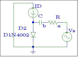
Fig # 3
Build the circuit shown in Fig # 3. R=R1 (1 W) and C=C1 (as large as possible)
- Set ID=14 mA, vs=15 mV rms, (100kHz sinusoidal signal), and measure va (or vs) and vb (or vd). Compute the small signal resistance of the diode for this operating point: rd = vd / id