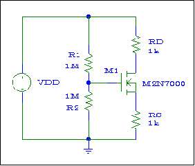
Figure # 1
Experiment # 9
Design of MOSFET
Amplifiers and Current Mirrors
Equipment:
You must make up a complete equipment
list and have your instructor review it before you start.
Objectives:
Figure # 1
1.- (HW) Design of Common Source
Design a Common Source voltage amplifier using circuit shown in Fig # 1.
Design Specifications of the Amplifier
|AV| > 15 (when loaded with RL= 1 k W )
RIN > 100 KW
Maximum Power Transfer must occur when loaded with RL= 1 k W (Use this info to find ROUT)
Vin max(before distortion) ³
60 mVpeak (when loaded with RL=1 k W)
2.- Assembly, Test and Verification of Specifications
Build and test your design. Measure and verify that your design meets all the given specifications.
a.Measure VG, VS, VD, and ID with no small signal input.
b.Measure Avo, Av@RL= 1K, Rin (input impedance) and Rout (output impedance) of the assembled circuit.
c.Find the maximum input voltage that the amplifier can accept before the output distorts.
d.Measure the phase
relationship between the input and output voltages.
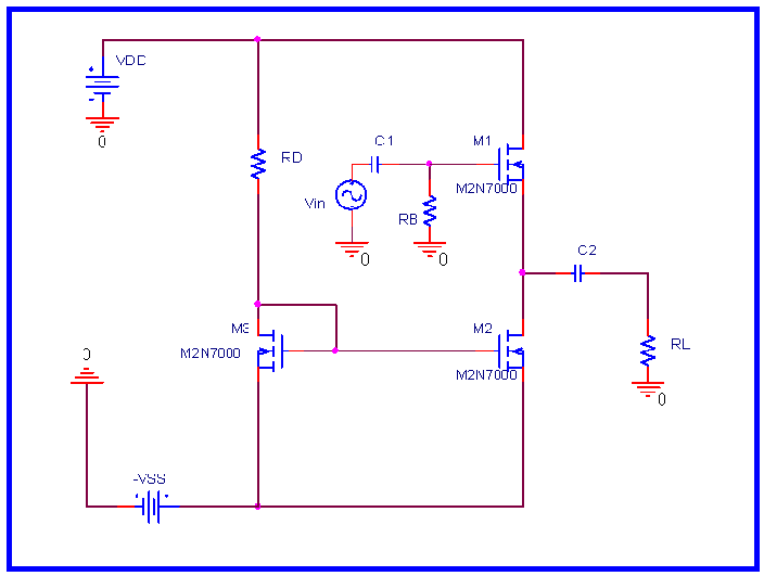
Figure # 2
3.- (HW) Design
Design a Common Drain voltage amplifier with current mirror similar to the one shown in Fig # 2.
Design Specifications of the Amplifier
ID = 15 mA
|AV| = 1 (when loaded with RL= 1 k W )
RIN ³ 500 KW
ROUT £ 100 W
4.- Assembly, Test and Verification of Specifications
Build and test your design. Measure and verify that your design meets all the given specifications.
a.Measure VG, VS, VD, and ID with no small signal input.
b.Measure Avo, Av@RL= 1K, Rin (input impedance) and Rout (output impedance) of the assembled circuit.
c.Find the maximum input voltage that the amplifier can accept before the output distorts.
d.Measure the phase
relationship between the input and output voltages.
5.- Analysis
a. Compare the measured results to your design calculations and specifications. Explain any and all differences.
b. Write equations and plot the AC and DC load line of Common Source and Common Drain. Explain how to pick a good point for CSC and CDC from the AC and DC load line. Example about picking good AC and DC line is in the lab handouts under "Design of Common Source/Drain" by Zvi Markowitz.
c. Is the current source design of the CDC (Fig. 2) a better choice compared to the configuration given in Fig. 1? If so, why?