The George Washington
University
School of Engineering
and Applied Science
Department of Electrical
and Computer Engineering
ECE 20 - Spring
2001
Experiment # 6 (Part
II)
Bipolar Junction
Transistors
Common Collector
(CC)
Equipment:
You must make up a complete equipment
list and have your instructor review it before you start.
Objectives:
-
To verify the small signal performance
for a given CCC amplifier: RIN, ROUT, Av, Ai , maximum input amplitude
without distortion vin max , etc.
-
To design an current amplifier according
to a set of specifications
-
To establish the relationship between
the voltage gain and the load
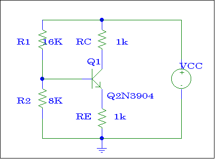
Figure # 1
1.- (HW)
Analysis
In Exp. #5, the DC Bias Analysis
and general formula for Unloaded Voltage Gain (Avo) for circuit of Figure
#1 were calculated. The more detailed analysis analysis on Common
Collector Amplifier for this circuit will be conducted in this section.
When this circuit is operated in
CCC:
-
Find ROUT
-
RIN
-
Unloaded Voltage Gain, Avo
-
Av (RL=ROUT)
-
Ai (RL=ROUT).
-
Maximum input voltage vin max that the
amplifier can accept before the output distorts (unloaded).
To get a credit for this analysis, you must show all the steps below:
1. Do DC Bias Analysis
2. Draw Small Signal Equivalent circuit for CCC
3. Find Rin, then Rout @Vin=0
4. Find Vout and Vin to get Av
5. Find Av @ RL=Rout
6. Find Ai
7. Find Vinmax
The text book and lab handout should give you a good example on how
to perform the analysis.
2.- Verification
Build and fully test the circuit
shown in Figure #1. By applying a sinusoidal signal such that the small
signal approximation holds, measure:
-
RIN (input impedance) and ROUT (output
impedance) of the assembled circuit. Read the lab handout to properly
understand how to measure Rin and Rout.
-
Unloaded Voltage gain, Avo. Label
the plot - "Plot 2a - Avo for CCC"
-
Voltage Gain for RL equal to 2*ROUT,
ROUT, ROUT /2, and ROUT /4. Print the output plot for each
case and label each plot as "Plot 2b - Av @ RL= [RL value] for CCC"
-
Find the maximum input voltage that
the amplifier can accept before the output distorts (Unloaded case). Print
the plot and label it as "Plot 2c - Vin max before output distorts for
CCC"
-
Determine the phase relationship between
the input and output voltages.
Hint: Connect a large capacitor
between VCC and ground in order to remove all the noise from the source.
The noise is amplified and mixes with the output due to the input AC signal
vs.
3.- (HW)
Design of Current Amplifier
In this section you are asked to
design a Current Amplifier. Current Amplifier is one application
of Common Collector. You can use Class A, Clas B or Class AB to design
your amplifier. Use ORCAD to verify that all the specifications have
been achieved.
Design Specifications of the Amplifier
VCC = 24 VDC ± 0.5 VDC
Vin = 250 mVsin
Ai = 20 @ 5 kHz
RL < 100 W
4.- Assembly, Test and Verification
of Specifications
Build and test your design. Measure
and verify that your design meets all the given specifications.
-
Measure all the necessary DC bias points
with no small signal input (Vs).
-
Connect the small signal input and measure
Av, Rin (input impedance) and Rout (output impedance) of the assembled
circuit (unloaded).
-
Find the maximum input voltage (Vin
max) that the amplifier can accept before the output distorts.
-
Measure the phase relationship between
the input and output voltages.
-
Print out the output plot of Vout and
Vin. Label this plot "Plot 4a - Design of CEC - Vout and Vin)".
Annotate
in the plot the Voltage gain Av you get from the circuit.
-
Use music as the Vinput and use speaker
as the R Load. What is your observation?
5.- Conclusion
-
Compare the measured results to your
design calculations and specifications. Explain any differences.
-
What can you say about the general characteristics
of CCC amplifier( Rin, Rout, Av, Ai etc)