Test Circuit #1
Experiment # 7
N-Channel Enhancement MOSFETs:
Testing &Characteristics
Equipment:
You must make up a complete
equipment
list and have your instructor review it before you start.
Components:
Q1 - 2N7000 MOSFET
R1 - 12 kW
R2 - 300 W
Objectives:
a) Refer to the specifications
for
the 2N7000 and find the following information:
transistor type,
the maximum total power it can
dissipate
at 250C (PD),
its maximum continuous drain current
rating (ID),
the maximum gate-source voltage
rating (VGS),
its operating temperature range
(TJ),
its maximum drain-source voltage
rating (VDSS),
its maximum zero gate voltage drain
current IDSS when VDS = 48 V & VGS = 0,
its maximum drain-gate voltage when
RGS = 1 mW,
its maximum static drain-source
on-resistance (rDS) when VGS = 10VDC & ID = 0.5 ADC,
its maximum and minimum gate
threshold
voltage (VGS(th)) when VDS = VGS & ID = 1mA,
its minimum forward transconductance
(gfs) when VDS = 10 V & ID = 200 mA,
its drain-source on-voltage
(VDS(on))
when VGS = 10 V & ID = 0.5 ADC,
and its minimum on-state drain
current
(ID(on)) when VGS = 4.5 V & VDS = 10 V.
--> Place all this information in Data Table A - 2N7000 Specifications & Ratings.
b) Identify the gate, drain and source pins of the 2N7000. Draw a pin out diagram of this device and call it Figure A - Pin Out Diagram of 2N7000.
c) Draw the internal circuit of the 2N7000 chip. Label this as Figure B - Internal circuit of the 2N7000 chip
d) Draw and label the electrical
symbols for a depletion N-Channel MOSFET and depletion P-Channel
MOSFET.
Draw and label the electrical symbols for an enhancement
N-Channel
MOSFET and enhancement P-Channel MOSFET. Place this information in Figure
C -Types of MOSFETs & Their Electrical Symbols.
2.- Static Measurements
a) Set the ohm meter to its
highest scale. Measure and record the resistance(R)
i)between the gate and source
ii)between the gate and drain
iii)between the drain and source.
Place this information in Data
Table B - 2N7000 Static Characteristics.
b) Based on the resistance values gotten from the measurement, do you think the MOSFET works properly? Explain.
c)Test the built-in diode
protection
of Q1 with the diode test feature found on the Keithley Model 175.
Measure and record the forward and
reverse biased readings of Q1. Include this information in Data Table B.
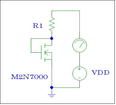
3.- Find VGS(th) when VDS = VGS & ID = 1 mA
Test Circuit #1
Assemble the circuit depicted
above
and then adjust VDD until the drain current (displayed on the ammeter)
is equal to 1.00 mA DC. Record the the value of VGS(th).
4.- Find VDS(on) when VGS = 4.5 V & ID = 75 mA
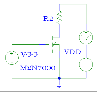
Test Circuit #2
Completely assemble this circuit
above; adjust VGG to 3.5 VDC and then adjust VDD until the drain
current
(displayed on the ammeter) is equal to 75.0 mADC. Record the value of VDS(on).
5- (HW) Transfer Characteristics ( ID vs. VGS) for different transistor parameters using ORCAD
With the help of ORCAD plot ID
vs.
VGS for VDS = 10 Volts DC. Vary the value of VGS in the 0 to 4 Volts
range.
Repeat this experiment for the
following
conditions:
a) b ( named ‘KP’ in ORCAD) is ten times its default value. Do not change the value of any of the other parameters. Make sure to LABEL simulation CLEARLY.
b) W (width of the transistor) is twenty times its default value. Do not change the value of any of the other parameters. Make sure to LABEL simulation CLEARLY.
c) tox ( gate oxide thickness ) is
twenty times its default value. Do not change the value of any of
the
other parameters.
Make sure to LABEL simulation CLEARLY.
d) Based on the simulation results, explain what happens to
the
graph of ID vs VGS when:
i) b value increase.
ii) W value increase.
iii) tox value increase.
6.- Find the Transfer Characteristic Curve (ID vs. VGS)
Using Test Circuit # 2: Place one
voltmeter between the drain and source of Q1 to measure VDS and place a
second voltmeter between the gate and source to measure the VGS of
Q1.
Completely assemble this circuit. Keep VDS set to 10 VDC while you step
VGG in 0.1 VDC increments starting at [ VGS(th) + 0.05 VDC ] and
stopping
[ VGS(th) + 1.05 VDC ]. Measure and record ID for each increment of
VGS.
Place this information in Data Table C - 2N7000 Transfer
Characteristic
Curve Data (ID vs. VGS). Make a plot using the data collected and
label
the plot "Plot 6a - ID vs VGS"
7.- ID vs. VDS Characteristics Using a Curve Tracer
Obtain a copy of a family of 10
curves
for the 2N7000 from the Tektronix Model 571 Curve tracer. Set ID to be
no greater than 50 mA, VDS to be no greater than 10 V, VG to step 10
times
in 0.1 V steps, the offset voltage to 0.05 V more than VGS(th) and Pmax
to .5 Watt.
Label the plot "Plot 7 - ID vs
VGS (Curve Tracer)"
8 - Analysis