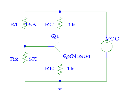
Figure # 1
Experiment # 4
Bipolar Junction Transistors:
DC Bias, BJT as Inverter and BJT as Amplifiers
Objectives:
Figure # 1
1.- (HW) DC Biasing Analysis
· Using simple
Kirchoff's Laws and Ohm's
Law, analyze the circuit shown in Figure # 1 and find VE, VC, VB ,VBE,
VCE, ,
IB, IE, IC, RB, (assume VCC = 30 VDC, b
= 180, VT = 26 mV).
Label this analysis - "Analysis #1 - DC Bias Calculation"
· Assemble this
circuit on ORCAD and
perform a bias point detail analysis. Use NS3904 for the BJT.
Show the
calculated voltages and currents by appropriately placing IPROBEs and
VIEWPOINTs on your schematic. Label the circuit as "Circuit
#1 -
DC Bias Simulation"
· Compare the DC Voltages and DC currents obtained from your hand calculation and ORCAD. Why there are some differences?
2.- (HW) Inverter Simulation
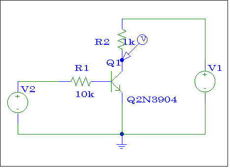
Figure # 2
Use SPICE to simulate the BJT inverter shown in Figure # 2. Use
NS3904 for
BJT. Plot the value of the output voltage VC vs.
the input
voltage V2. Label this plot as "Plot #1 -Inverter
Simulation". V1 is 5 VDC. Use "DC Sweep" to
set V2 from 0 to 5 Volts with an increment of 0.5 VDC.
Indicate in the plot when the BJT is in the saturation, linear, or
cut-off
region.
3.- Verification for DC Biasing and Inverter
4. - (H/W) Analysis of BJT as an Amplifier
In analog circuit, BJT is used primarily in the amplification
circuit.
There are three basic amplifier configurations and each configuration
has a
specific application to electrical circuit. The configurations
are:
1) Common Emitter
2) Common Collector
3) Common Base
Further information can be read from the textbook in Chapter 5.7.
Using circuit of Figure #1, derive a formula and find the values
for:
i) Voltage Gain of Common Emitter
ii) Voltage Gain of Common Collector
iii) Voltage Gain of Common Base
Hint: To derive the voltage
gain for
each configuration, you need to follow these steps:
1) Do a DC Bias Analysis (which you already did in Part 1)
2) Draw a small signal analysis corresponding to each
configuration. For
example small signal analysis for
CEC is different from small signal analysis for CCC.
3) Find the expression for Voutput
and Vinput.
4) Voltage Gain = Voutput /
Vinput.
5. - Verification of BJT as an Amplifiers
b) By applying a sinusoidal signal (small signal) as the input, measure:
Important Hints:
There are several steps that you must do to ensure proper small
signal
measurement:
1. Connect a large capacitor between VCC and ground in order
to remove
all the noise from the source.
2. Use a really small sinusoidal signal as your input. Vinput < 100mVp.
3. Check your DC Bias Voltages and Currents before measuring the
small
signal. Make sure that the BJT is operating in the correct
Bias
Point (DC) before doing any small signal measurement. For
example, VBE
must be at least 0.6 VDC.
4. Use Vpp option in the oscilloscope to measure the Voutput and Vinput.
6.- Conclusion
Write a clear conclusion establishing the most important facts about
the
operation of the BJT inverter, the beta stabilized biasing network and
particularly its operation in the different configurations.