The George Washington University
School of Engineering and Applied Science
Department of Electrical and Computer Engineering
ECE 20 - Fall 2005
Experiment # 3
Bipolar Junction Transistors
Testing & Characteristic
Equipment:
You must make up a complete equipment
list and have your instructor review it before you start.
Components:
-
Q1 - 2N3904 NPN Transistor
-
R1 - 100 KW
Objectives:
-
To use an ohm meter to determine the forward
and reverse resistance of transistor pn junctions
-
To use the diode test function of the Keithley
Model 175 to measure transistor pn junction characteristics
-
To obtain several transistor characteristic
curves by plotting the information taken from a transistor test circuit
-
To obtain the IV Characteristic Curves
for a transistor by using a Tektronix Model 571 Curve Tracer
-
To determine the h parameters (hie,
hre, hfe and hoe) of a Transistor
-
To verify manufacturer specifications
1.-
(HW) Transistor specifications, ratings and symbols
Refer to the specifications
for the 2N3904 and find the following information. The specification
(in PDF format) can be accessed HERE.
-
transistor type
-
maximum power it
can dissipate at 250
Celcius
-
maximum collector
current rating
-
maximum collector
to emitter voltage rating
-
operating temperature
range
-
minimum and maximum
hfe
-
the emitter to base
breakdown voltage
-
hie @
IC = 5 mA
-
hfe @
IC = 5 mA
-
hoe @
IC = 5 mA
-
hre @
IC = 5 mA
-
VBE @
VCE = 1.0 V and IC = 5 mA
-
Place all this information
in Data Table A - 2N3904 Specifications & Ratings.
-
Identify the base,
collector and emitter pins of the 2N3904. Draw a pin out diagram of this
device and call it Figure A - Pin Out Diagram of 2N3904.
-
Draw and label the
electrical symbols for a NPN and PNP transistor. Place this information
in Figure B - Types of Transistors & Their Electrical Symbols.
2.- Static Measurements
-
(HW)
From experiment #1, what would you think the forward-biased Resistance
values are for base-emitter junction and the base-collector junction
of Q1 ?
-
Set the ohm meter to the 200 kW
scale. Measure and record the forward bias resistance of the base-emitter
junction and the base-collector junction in Q1. Set the ohm
meter to its highest scale and measure and record the reverse bias resistance
of both junctions in Q1. Place this information in Data Table
B - 2N3904 Characteristics.
-
(HW)How
do you make sure that the base-emitter or base-collector pn junctions were
working properly using Keithley Model 175.
-
Test both pn junctions of Q1
with the diode test function of the Keithley Model 175. Measure and record
the forward and reverse biased readings of Q1 of both of these
junctions. Include this information also in Data Table B.
3.- (HW)
IB vs VBE for different values of VCE
with ORCAD
Plot IB
vs VBE for different values of VCE. Use Figure #1
for the circuit. This plot is a SPICE parametric DC sweep. The ranges
for IB and VBE are 50 mA
and 1Volt. VCE should vary from 0 to 10 Volts with 1 Volt increments.
Label this plot "Plot A - ORCAD IB vs VBE".
Hint: NS3904
can be obtained from "bipolar.olb" library in ORCAD. You must do
DC sweep with primary sweep varying VBE and secondary Sweep
varying VCE. IB should be in y axis.
4.- IB vs VBE
Measurements Using a Test Circuit
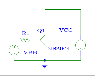
Fig # 1
Assemble the circuit shown in Figure
# 1.
a) Set VCE = 1 VDC
and vary IB from 5 to 50 mA
in steps of 5 mA
and record the values of IB and VBE for each
step.
b) Set VCE = 10 VDC
and once again vary IB from 5 to 50 mA
in steps of 5 mA
and record the value of IB and VBE for each
step.
Place all this information in Data
Table # 1 - Base Characteristics. Plot IB vs. VBE
in Graph # 1 - 2N3904 Base Characteristics (be sure to annotate
the VCE lines for VCE = 1V and VCE = 10V).
5.- (HW)
IC vs VCE for different values of IB with
ORCAD
-
Plot IC
vs VCE for different values of IB. Use Figure #1
for the circuit. This plot is a SPICE parametric DC sweep. The ranges
for IC and VCE are 10 mA and 10 Volts. IB
should vary from 0 to 50 mA
with 5 mA
increments. Label this plot "Plot B- ORCAD IC vs VCE".
-
Repeat part a) but
for the value of b
equal to 10. Why there is a difference in the graph when you change b
value?
Hint: To change
b
value, follow these steps:
1. Highlight
NS3904 in the circuit
2. Click
on Edit
3. Click
on PSpice Model.
4. b is
called "BF" in the model.
5. Change
the BF value to 10
Hint: NS3904 can be obtained from "bipolar.olb"
library in ORCAD. You must do DC sweep with primary sweep varying
VCE and secondary Sweep varying VBE. IC
should be in y axis.
6.- IC vs VCE
Measurements Using a Test Circuit
Using circuit of Figure #1:
a) Set IB = 20 mA
and vary VCE from 0 to 2 VDC in 0.2 VDC
steps. Then vary VCE from 2 VDC to 10 VDC
in 2.0 VDC steps. Record the value of IC
and VCE for each step.
b) Set IB = 40 mA
and vary VCE from 0 to 2 VDC in 0.2 VDC
steps. Then vary VCE from 2 VDC to 10 VDC
in 2.0 VDC steps.
record the value of IC
and VCE for each step.
Place all this information in Data
Table # 2 - IV Characteristic Data. Plot IC vs. VCE
in Graph # 2 - 2N3904 Characteristic Curves (be sure to annotate
the IB lines for IB = 20 mA
and IB = 40 mA).
7.- IC
vs VCE Measurements Using a Curve Tracer
Obtain a copy of a family of 10 curves
for the 2N3904 from the Tektronix Model 571 Curve tracer. Set IC
to be no greater than 10 mA, VCE to be no greater than 10 V
and IB to step 10 times in 5 mA
steps (be sure to annotate the IB lines). Label this plot
as "Plot C - IC vs VCE Measurements Using a Curve
Tracer"
8.- Data Analysis
-
Determine hie, hre,
hfe, and hoe when VCE = 5V and IC
= 5 mA from Graph #1 and Graph #2.
Hint: Use the handout that will
be given in class to find those values.
-
Compare your results to the manufactures
specifications.
-
Determine the values of gm,
rp,
re, and ro in terms of the h parameters.
-
Determine the values of gm,
rp,
and re from the following formulas:
gm= IC / VT
rp=
VT / IB
re= VT / IE
-
Compare the values obtaine in c) and d)