The George Washington University
School of Engineering and Applied
Science
Department of
Electrical and Computer Engineering
ECE 20 - LAB
Experiment # 9
CD amplifier with Current Mirror, CMOS Inverter, NAND, and NOR Gate Design
Equipment:
You must make up a complete equipment list and have
your instructor review it before you start.
Objectives:
- Designing a Common Drain voltage amplifier with current mirror
- To test a CMOS inverter using the 4007 MOS array chip
- To simulate a CMOS inverter using the IRF9140 and IRF150 MOS transistors in SPICE
- To design a CMOS NAND gate and a CMOS NOR gate both using 4007 MOS chip and using the IRF9140 and IRF150 MOS transistors in SPICE
- To compare propagation delays of these gates.
1. Designing a Common Drain voltage amplifier with current mirror
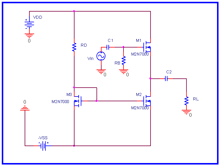
1a).- (HW) Design
Design a Common Drain voltage amplifier with current mirror similar to the
one shown in Fig # 2. Use SPICE to verify that all the specifications have been
achieved.
Design Specifications of the Amplifier
VDD = ± 9 VDC
ID = 50 mA
|AV| = 1 (when loaded with RL= 1 k W )
RIN ³ 2 MW
ROUT £ 100 W
Vout max (before distortion) ³ 4 Vpeak (loaded with RL=1kW)
- Show all design calculations.
- Compare the SPICE results to your design calculations and specifications and explain any and all differences.
1.b).- Assembly, Test and Verification of Specifications
Build and test your design. Measure and verify that your design meets all the given specifications.
a. Measure VG, VS, VD, and ID with no input.
b. Measure Avo, Av(RL @ max power transfer), Rin (input impedance) and Rout (output impedance) of the assembled circuit.
c. Find the maximum input voltage that the amplifier can accept before the output distorts.
d. Measure the phase relationship between the input and output voltages.
2.- (HW)Inverter Simulation
- Simulate (PSPICE) a CMOS inverter built utilizing a PMOS IRF9140 and an NMOS IRF150 for the K parameter of the p transistor (Kp) being equal to K parameter of the n transistor (Kn). Repeat the simulation for Kp = 4 Kn, Kp = 2 Kn, Kp = 0.5 Kn, and Kp = 0.25 Kn. Compare the output graphs and comment on each case. Use VDD=0 Volts and VSS=10Volts.
- Simulate the same circuit for the temperature values of 100K, 300K, and 500K, separately. Compare and comment on the output graphs.
- Connect 100 nf load capacitor to the output of the circuit .Simulate this circuit for Kp = 4Kn , Kp= 2Kn, Kp= 0.5 Kn and Kp = 0.25 Kn and measure low-to- high and high-to-low propagation delay of the inverter for each case.
- Connect one more CMOS inverter in series and measure low-to- high and high-to-low propagation delay again of the first inverter in the sequence.
- Compare the values with those obtained in part (c) and comment on the load capacitance of the second inverter.
3.- Verification
Completely assemble the CMOS circuit using the 4007 MOS array chip. Place one voltmeter between the output and the ground of the circuit to measure the output voltage vout. Keep VDD set to 10 while you step vin in 0.5 Volt increments from 0 to 4, in 0.25 Volt increments from 4 to 6 and in 0.5 Volt increments from 6 to 10.
a) Measure the output voltage for each increment of vin.
b) Measure the drain current and find the input voltage value when drain current is maximum (at this voltage value be vm).
c) Measure the input voltage vin when it is equal to output voltage vout. Check whether this value is close (or equal to) vm measured in part b.
d) Write a comment on the drain current vs. input voltage characteristics.
4.- CMOS Logic Gate Design ( Where digital electronics
begins)
a) NAND gate design:
- Design a NAND gate using the 4007 CMOS chip. Apply two 10Volt square-wave signals operating at different frequencies to observe the output vs. input characteristics. One frequency must be twice the value of the other.
- Make the same design in SPICE using IRF150 and IRF9140 transistors and plot the output vs. input voltage characteristics.
- In SPICE, connect a 100nf capacitor to the output of the NAND gate, and measure low-to-high and high-to-low propagation time delays of the NAND gate. Repeat the same experiment for 100pf, 1µf, and 10µf capacitors. What kind of relation can you observe between load capacitance and propagation delay of the gate.
b) NOR gate design:
- Design a NOR gate using the 4007 CMOS chip. Apply two 10Volt square-wave signals operating at different frequencies to observe the output vs. input characteristics. One frequency must be twice the value of the other.
- Make the same design in SPICE using IRF150 and IRF9140 transistors and plot the output vs. input voltage characteristics.
- In SPICE, connect a 100nf capacitor to the output of the NOR gate, and measure low-to-high and high-to-low propagation time delays of the NOR gate. Repeat the same experiment for 100pf, 1µf, and 10µf capacitors. What kind of relation can you observe between load capacitance and propagation delay of the gate.
c) Comparison:
Compare the propagation delays of NAND, NOR and Inverter gates when load capacitor is 100nF. Which one is the fastest? Why? (Bonus will be given to those who can explain the reason mathematically)