The George Washington University
School of Engineering and Applied Science
Department of Electrical and Computer
Engineering
ECE 20 - LAB
Experiment # 2
Solid
State Diodes
Applications I
Equipment:
You must make up a complete equipment list and have you instructor review it
before you start.
Components:
- D1 through D2 - 1N4002
- T1 - 12.6 - 16.0 Volt Center Tapped Transformer
- R1 - 16 kW
- C1 - C2 - capacitors, to be determined by your voltage doubler design
- R2 resistor, to be determined by your voltage doubler design
Objectives:
- To measure the output characteristics of your transformer
- To build and safely test a half wave rectifier
- To build and safely test a full wave rectifier
- To build and safely test a bridge rectifier
- To design, build and test a voltage doubler
CAUTION!
BE CAREFUL DURING THIS EXPERIMENT!
HAZARDOUS VOLTAGES WILL
BE PRESENT WHEN YOU PERFORM
YOUR MEASUREMENTS!
1.- Types of Positive Voltage Rectifiers (HW)
A. Draw and label the following types of positive voltage rectifiers (use PSPICE schematic module):
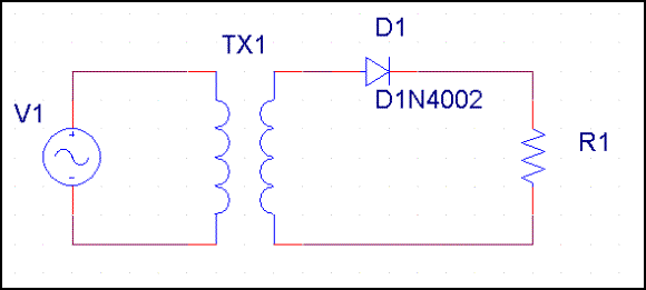
a. Figure #1 -- Half Wave Rectifier
b. Figure
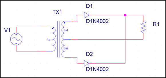
#2 – Full Wave Rectifier
c.
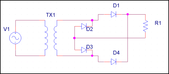
Figure #3 -- Bridge Rectifier
B. Designate the transformer as T1, the load as R1 and the rectifier diodes as D1, D2, D3 and D4.
C. With the help of SPICE, run a transient simulation for
each of them, and plot 10 complete cycles of the input
signal/signals and the
corresponding output signal.
D. Indicate in the different regions of each of the output
signal plots the function performed by each of the diodes of the
corresponding rectifier, and any
relevant details.
2.- The Turns Ratio
WARNING - Hazardous voltages will be present!
- Connect T1 to an AC outlet located on your bench. Use the Keithley Model 175 to measure the transformer primary voltage (V1) and secondary voltage (measure voltage between orange and white cable) (V2). Determine the turns ratio (V1/V2) of T1 and express the primary and secondary in VPP, VP, Vrms and Vavg. Place this information in an appropriate data table (Table # 1).
- Connect the oscilloscope only to the secondary! Never connect the scope to the primary! The negative lead on the scope probe is ground. If you connect this lead to the primary, you will cause 120 Vrms at 20 Amps to short through your probe to ground! Use the scope to measure the details of waveform present across the secondary winding. Label this plot Figure A - Unloaded Transformer Secondary Waveform. Disconnect T1 from the AC outlet!
3.- Testing Positive Rectifiers
WARNING - Hazardous voltages will be present!
- Construct the circuit shown
in Figure #1. Test the circuit for a possible short to ground with an ohm
meter. Correct any wiring errors and test again. Connect T1
to an AC outlet. Measure and record the wave form across R1. DisconnectT1
from the AC outlet! Plot and label the waveform Figure 1A -- Wave Form
Across R1 In Half Wave Rectifier. Indicate and measure any relevant
detail.
WARNING - Hazardous voltages will be present!
- Construct the circuit shown
in Figure #2. Test the circuit for a possible short to ground with an ohm
meter. Correct any wiring errors and test again. Connect T1 to an
AC outlet. Measure and record the wave form across R1. Disconnect T1
from the AC outlet! Plot and label the waveform Figure 2A -- Wave Form
Across R1 In Full Wave Rectifier. Indicate and measure any relevant
detail.
WARNING - Hazardous voltages will be present!
- Construct the circuit shown
in Figure #3. Test the circuit for a possible short to ground with an ohm
meter. Correct any wiring errors and test again. Connect T1 to an
AC outlet. Measure and record the wave form across R1. Disconnect T1
from the AC outlet! Plot and label the waveform Figure 3A -- Wave Form
Across R1 In Bridge Rectifier. Indicate and measure any relevant detail.
4.- Voltage Doubler Design
- (HW) Design and build
a voltage doubler that has the specifications below. Draw and label the
schematic Figure # 4 - Voltage Doubler (use PSPICE schematic module). With
the help of SPICE, run a transient simulation, and plot 10 complete cycles
of the input signal, signal accross each of the diodes, and accross each
of the capacitors. Be sure that your design guarantees that steady state
is reached in less than 10 cycles.
- Build the design in part a) and plot the real signals corresponding to those obtained in part a).input and output.
- Input: 12 Vp (output of your transformer)
- Output: 24 VDC
- Type of Load: resistive
- Power to Load: 100
mWDC
- WARNING - Hazardous voltages will be present!
5.- Analysis of results
- Compare the measured results
of each type of positive rectifier to those obtained using PSPICE. Include
in your comparison all waveforms and details that you measured.
- Compare each positive
rectifier to each other and detail the characteristics of each.
- Explain the theory behind the voltage doubler you designed. Show all waveforms and explain what each component does.